
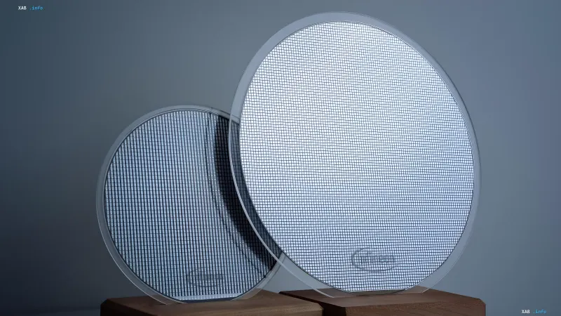
German company Infineon Technologies has announced a significant technological milestone in the field of power semiconductors: the company has successfully produced functional silicon carbide (SiC) chips on 300mm diameter silicon wafers. The tests were conducted at its plant in Villach, Austria, using equipment already employed for the production of standard silicon chips. According to Infineon, this marks the first such demonstration in a full-scale industrial production environment, rather than a laboratory setting. Moving to larger wafers allows for 2.3 times more chips per wafer compared to the existing 200mm format, which directly impacts the unit cost of each die.
Compatibility with existing equipment is a key factor
Crucially, Infineon did not need to purchase a new specialized fleet of machines to work with 300mm silicon carbide wafers. Utilizing existing production equipment, honed over years of silicon chip manufacturing, significantly lowers the entry barrier for the new format and simplifies production scaling. This means the company can increase capacity without the level of capital expenditure typically required when transitioning to fundamentally new technology nodes.
Cold Split technology tested in Dresden
In parallel with the tests in Villach, Infineon validated the Cold Split technology on 300mm silicon carbide wafers at its site in Dresden. Cold Split allows for separating thin wafers from the source crystal faster and with less material loss compared to traditional mechanical sawing. Combined with compatibility with existing equipment, this paves the way for further cost reductions and simplified scaling. The company stated it intends to continue developing the technology and discussing implementation timelines with partners for serial production, while maintaining development of the existing 200mm wafer line.
Target markets: from electric vehicles to AI data centers
Power components based on silicon carbide are in high demand for electric vehicles, charging stations, energy storage systems, and industrial equipment. They enable more efficient power conversion and can withstand high voltages and temperatures, which is critical for next-generation power electronics. Another promising area identified by Infineon is data centers for artificial intelligence, where such chips can be used in power supplies, solid-state transformers, and circuit breakers. Growing power consumption in AI infrastructure makes this segment one of the most dynamic for SiC components.
Context and outlook
Infineon's demonstration in November 2026 highlights the semiconductor industry's broader trend of transitioning to larger wafers for a wide range of materials, including silicon carbide and gallium nitride. Increasing the diameter from 200 to 300 mm is a standard step for the silicon industry, but for SiC—where crystallization and material processing are significantly more complex—this transition requires dedicated engineering efforts. Successful completion of an industrial test using existing equipment puts Infineon in an advantageous position relative to competitors, who may require longer adaptation cycles for their production lines.