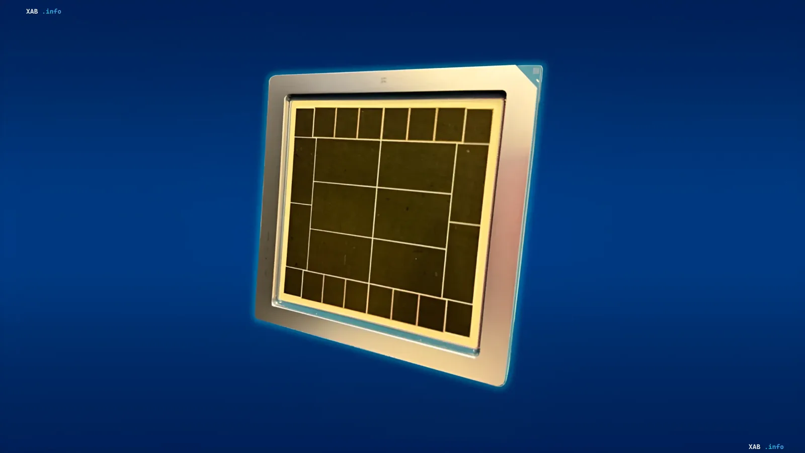
Intel has announced a critical milestone in semiconductor manufacturing. The American giant has demonstrated the ability to create chips of unprecedented size, opening new horizons for the development of artificial intelligence infrastructure. According to ixbt.com, this is not about classic monolithic crystals, but about advanced chiplet solutions and innovative packaging technologies.
Silicon mosaic instead of a monolith
Intel's production facilities in Rio Rancho (New Mexico) have become a testing ground for technologies capable of radically changing the landscape of microelectronics. Engineers have managed to significantly expand the maximum size of the photomask. This allows the package dimensions to be increased eightfold compared to current industrial standards. In the future, by 2028, this figure could exceed a twelvefold increase.
Company specialists describe the new approach as creating a "silicon mosaic." In this concept, specialized elements are interconnected to form a single massive package. Ultra-large solutions based on the new technology will reach dimensions of 240 by 240 millimeters. This step will ensure a 24-fold increase in photomask volume, significantly surpassing all previous industry indicators.
Victory over deformation physics
One of the main challenges in creating chips of such scale is the physical integrity of the substrate. On such a large area, deformations inevitably arise that can disrupt the operation of the microcircuit. Intel engineers have successfully tackled this problem by developing methods for stress compensation.
This success is directly related to market competition. For reference: due to difficulties with physical strength and deformation, other major players, including NVIDIA, were forced to abandon the creation of the Rubin Ultra chip, which was planned to be placed with two GPUs on a single substrate. Intel's ability to overcome these barriers puts the company in a unique position.
A new chapter for artificial intelligence
Such large-scale and complex structures are necessary primarily to meet the needs of the rapidly developing AI market. Intel's advanced technologies allow placing several compute chiplets and numerous memory chips directly on a single substrate. This ensures high performance and a sharp increase in the efficiency of subsystems designed for artificial intelligence tasks. Thus, Intel engineers are opening a completely new chapter in the microelectronics industry.