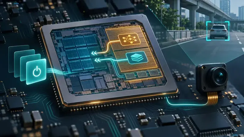
While the cloud can solve problems of any complexity, in challenging driving conditions, it is best to rely solely on yourself. For precisely such scenarios, Aisin — the world's largest automotive parts manufacturer — in collaboration with researchers from Tohoku University, has developed a specialized artificial intelligence accelerator focused on onboard image recognition. The chip was presented on November 2, 2026, at the IEEE Asian Solid-State Circuits Conference 2026. According to the company, the microcircuit consumes approximately 50 times less energy than traditional architecture during data processing, which corresponds to roughly a 98% reduction in power consumption and a 90% speedup in operations.
Architecture: Non-Volatile Memory and Near-Memory Computing
A key feature of the development is the use of non-volatile STT-MRAM (Spin-Transfer Torque Magnetoresistive Random Access Memory), which retains data thanks to the magnetic properties of the material even after power is turned off. Unlike the classical setup with external storage and DRAM, the new System-on-Chip (SoC) stores both neural network model weights and operating system boot data directly on the die. This eliminates the need to transfer large volumes of data from external memory upon device startup. Developers call this approach Near-Memory Computing (NMC) because it reduces data movement between computing units and storage.
Process Node and Layout: 16nm and 32MB of Embedded Memory
Notably, the chip did not require cutting-edge process nodes: it is manufactured using 16nm FinFET production standards. The embedded STT-MRAM has a capacity of 32MB. This choice allows for a compact and energy-efficient solution for onboard applications without relying on the most expensive lithography nodes, which is crucial for mass-market automotive electronics.
Test Results: Tiny YOLOv3 and Hundreds of Milliseconds to First Recognition
To verify the microcircuit's capabilities, the Tiny YOLOv3 neural network, designed for object detection in images, was used. To fit the model into the limited embedded memory volume, engineers applied a hybrid architecture and shared weight coefficients. As a result, the time from power-on to operating system startup was 65.7 ms — 38.59 times faster than a traditional system with external memory. AI processing time itself was reduced by 10.16 times, and the total time from startup to the completion of the first recognition dropped roughly 25-fold to 124.2 ms. Separately, the developers reported object detection energy costs of 50.7 mJ per frame, which is approximately 1/50th of the figure for the comparable traditional system.
Important Caveats: Prototype and Unspecified Manufacturer
It is important to emphasize that the claimed 98% applies not to all artificial intelligence computations or the power consumption of all existing processors, but to a specific experiment with Tiny YOLOv3 and the matched memory configuration. Furthermore, this is currently an experimental development rather than a mass-production processor: Aisin and Tohoku University have not announced a timeline for mass production or specific commercial devices that will use the microcircuit. The official manufacturer of the chip has also not been named; however, Taiwanese sources have linked Aisin's development to TSMC.