
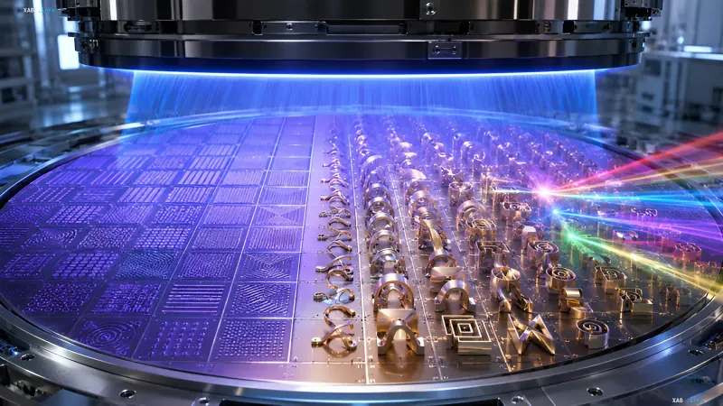
In the world of microelectronics and photonics, production speed often becomes the main bottleneck for implementing new technologies. Ion-beam lithography, despite its ability to create chips with extremely small process nodes, has traditionally lagged behind photolithography in productivity. However, Chinese researchers have presented a method that radically changes the situation, accelerating the processing of silicon wafers by hundreds of times.
Breakthrough at the CAS Institute of Physics
A group of scientists from the Institute of Physics of the Chinese Academy of Sciences (CAS), together with colleagues from the University of Hong Kong and other organizations, has developed a method for the mass formation of three-dimensional elements of photonic chips. The results of the work, published in the journal Advanced Materials, demonstrate a reduction in the time of the main manufacturing stage from several hours to tens of seconds.
The key achievement was the simultaneous transformation of flat nanostructures across the entire surface of a 10-centimeter (4-inch) wafer in a single pass. Researchers ensured the uniformity of bends for more than 97% of the manufactured nano-elements, which opens real prospects for transitioning to mass industrial production.
"Ion Origami" Technology
The new technique is called "ion-beam-induced origami." The process begins with the creation of flat blanks on silicon nitride membranes using electron lithography, which are then coated with a layer of gold. The next stage is irradiating the wafer with a wide parallel beam of argon ions.
Ions create defects and internal mechanical stresses in the near-surface layer of the material. Under their influence, pre-prepared elements bend synchronously, transforming into specified three-dimensional structures. In experiments, two-layer elements with a thickness of about 50 nm each were used, and the formation of arrays took approximately 20 seconds.
Parallel Processing vs. Sequential Processing
In classical ion-beam lithography, a focused beam processes structures sequentially, point by point. Even a small area of 100 × 100 µm can require up to seven minutes for processing, and creating large arrays takes hours. Chinese scientists replaced this approach with the use of a wide beam that acts on all elements in parallel.
Thanks to this, the transformation time decreased by more than one hundred times and practically ceased to depend on the number of elements on the wafer. It is important to note that this refers to the acceleration of the specific stage of structure formation, whereas the full cycle of photonic chip production, naturally, will take more time.
Practical Application and Prospects
To demonstrate the effectiveness of the technology, scientists created two types of devices. The first was a three-dimensional chiral metasurface for circular polarization tasks. It showed a circular dichroism of 0.8 at a wavelength of 3.41 µm, indicating a high ability to distinguish between left and right circular polarization.
The second example was a bendable plasmonic grating. When its curvature is changed, the resonance retunes by more than 150 nm in the visible region of the spectrum. Such structures can find application in polarization sensors, spectral filters, optical communication networks, and integrated photonic circuits. In the future, researchers plan to evaluate the industrial suitability of the method by studying the defect rate, circuit durability, and process cost.