
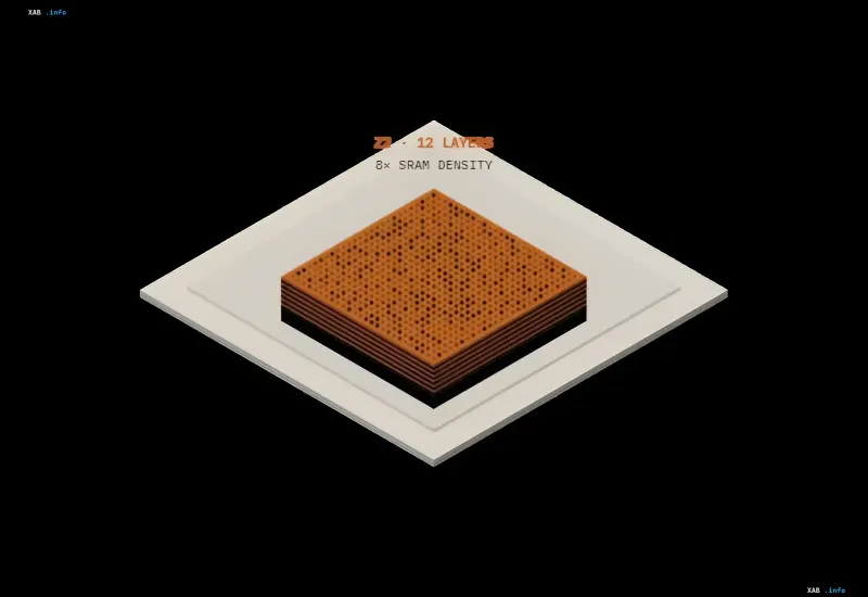
Former Intel CEO Patrick Gelsinger invested personal capital last year into startup Nagare Labs, which is developing a new class of memory called Z2RAM. According to its creators, this type of memory is designed to combine the best properties of three established technologies: the packing density typical of DRAM, operation speed comparable to SRAM, and scalability close to flash memory. As Gelsinger explained to The Register, the memory market has not seen fundamental innovations over the past three decades—all developments revolve around the same triad of SRAM, DRAM, and flash memory—which is why the emergence of an alternative approach is generating heightened interest among investors and manufacturers.
Technological Foundation: Oxide Semiconductors and 3D Bonding
Nagare Labs' technology is built on oxide semiconductors and involves integrating memory directly into computational components using 3D bonding techniques. Conceptually, Z2RAM resembles the 3D V-Cache memory that AMD places on some of its Ryzen processors: an additional memory layer is added to the logic chip packaging, increasing the available third-level cache volume. At the same time, according to Nagare Labs representatives, Z2RAM is closer to SRAM in speed, and closer to DRAM in its data storage mechanism: unlike a DRAM cell consisting of a single transistor and capacitor, a Z2RAM cell contains two transistors, using the gate capacitance of the second to store charge, which reduces read latency.
Density: Over Five Times Higher Than SRAM on the Same Die
In its first iteration, Z2RAM promises a bit-density more than five times higher than that of SRAM. If an SRAM die places about 64 MB of memory in a given space, Z2RAM offers around 320 MB in the same volume while maintaining bandwidth at a level comparable to SRAM. Such capacities are unimpressive against the background of flagship accelerators with HBM memory, but for SRAM-based accelerators like Nvidia Groq, this could be a significant step forward: Groq 3 LPU-type chips offer about 500 MB of SRAM, and with the transition to Z2RAM, this volume could theoretically grow fivefold or more.
Manufacturing: Simpler Than HBM, But Currently Lab-Only
The vertical multi-level layout of Z2RAM formally resembles HBM, but from a manufacturing technology standpoint, it is closer to forming layers in NAND chips, which, according to the startup's assessment, makes it significantly cheaper than HBM and easier to manufacture. At the same time, Gelsinger acknowledges that in the "density plus speed" pairing, HBM remains the best on the market today, albeit with limitations on density, power consumption, and bandwidth at the chip's peripheral areas. Z2RAM prototypes have not yet left the laboratories, so Nagare Labs is looking for a partner with a pilot production line to release the first samples. The company plans to obtain working chips within four years and establish mass deliveries of serial units within the next decade.
Risks: Lack of Standard and Oxide Instability
The company is ready to cooperate with third-party chip developers wanting to integrate Z2RAM into their components, but two obstacles stand in this way. The first is the lack of a standard interface: the startup could develop it independently, but this is a complex task. The second is the low stability of oxide semiconductor product properties, which complicates manufacturing scaling. According to Nagare Labs representatives, strict industry standards have already "buried" quite a few developments in new memory types, but the market is simultaneously opening up new opportunities. Gelsinger notes that the artificial intelligence boom has revealed an acute need for both bandwidth and memory capacity used in existing infrastructure, which is why enormous interest persists in breakthrough developments in this area, accompanied by capital resources to stimulate them.