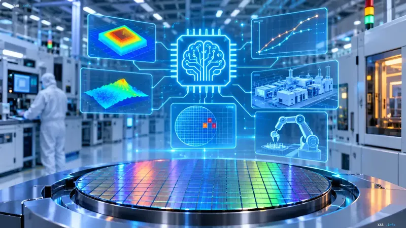
Behind the release of any mass semiconductor product lies a colossal layer of engineering work: at the stage of designing technological processes and the chips themselves, R&D employees make decisions that subsequently determine both the characteristics of the finished dies and the defect rate in production. It is at this exact point that Nvidia has placed its bet on artificial intelligence, introducing the concept of so-called AI-defined fabs—semiconductor factories managed by AI. The company emphasizes that this does not yet involve fully autonomous enterprises, although in the long term the industry will indeed arrive there. At the current stage, the focus has shifted to integrating neural network models into process design, physical phenomenon simulation, quality control, and production line management.
Accelerating Physical Simulation: From Heat Transfer to Lithography
One of the key areas of the concept is accelerating multi-physics simulation, which simultaneously accounts for heat transfer, electrical processes, and mechanical stresses in silicon structures. A concrete example has already been implemented: COMSOL uses the Nvidia cuDSS library to accelerate such calculations during the development of semiconductor equipment and technological processes. The claimed performance boost reaches up to ten times compared to traditional CPU-based solutions. A similar approach is applied in atomic-level materials modeling: the Applied Materials Ginestra platform, built on cuDSS, works up to ten times faster than purely processor-based counterparts, while the ACE+ system using PhysicsNeMo accelerates surface topography formation modeling up to 35 times. In the field of lithography, Siemens is integrating the cuLitho library into its Calibre software, achieving speedups of up to 17 times for individual computational tasks.
Milliseconds Instead of Days: AI Forecasting Instead of Full Calculation
The second approach is fundamentally different: instead of re-running full computational simulations, AI models trained on the results of physical simulations are used. This makes it possible to predict the behavior of technological processes solely through prediction, which saves resources on conducting expensive verifications on active production lines. The most telling example is Lam Research, which applied Nvidia PhysicsNeMo to predict plasma behavior during the plasma etching of silicon wafers. Such calculations require taking into account the interaction of electrical, chemical, and thermal processes. According to Nvidia, the trained model generates a forecast in milliseconds, whereas a full-fledged real experiment or repeated calculation would take several days. Virtually, this resembles a form of intuition, although in the context of industrial AI, talking about intuition is premature.
AI Agents and Factory Digital Twins
At the level of testing and production management, the concept is complemented by AI agents and digital twins. Advantest uses Nvidia NeMo Switchyard agents to automatically select appropriate AI models when analyzing semiconductor test results: according to Nvidia, this reduces the execution time of corresponding operations from several hours to a few minutes. Applied Materials, in turn, creates digital twins of entire factories using Nvidia Omniverse libraries. In a virtual environment, engineers can simulate material movement, equipment placement, section productivity, and potential bottlenecks, testing changes before implementing them in a real enterprise.
The Engineer Remains in the Control Loop
According to Nvidia's vision, taken together, the promoted processes of transferring a number of key engineering duties to artificial intelligence create the basis for a new approach to microchip manufacturing. At the same time, engineers retain control over technological decisions but receive analysis results much faster. Ultimately, as the company positions it, this will allow for faster release of higher-quality electronics and computing equipment, shortening the cycle from design to mass production and minimizing the number of costly experiments directly on the production line.