
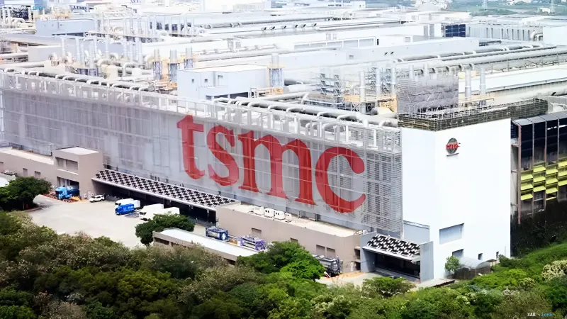
Taiwanese TSMC, the world's largest contract semiconductor manufacturer, continues to roll out its advanced 1.4-nanometer process technology, internally designated as A14. According to industry publication DigiTimes, the company intends to transition to mass production of chips using this process by the first half of 2028, with its production capacity potentially exceeding Intel's figures for the competing 14A process by 7.5 times. Both technologies represent a crucial milestone in the battle for the advanced processor market, and the stated timelines and specifications currently fall under the company's plans and preliminary data.
Timeline: From Risk Production to Mass Manufacturing
Before mass production, TSMC expects to transition to so-called risk production in the second half of 2027, which allows the process to be tested on real orders before full line deployment. Fab 20 in the Hsinchu Science Park and Fab 25 in Central Taiwan are expected to shoulder the main workload at this stage. Meanwhile, several Taiwanese sources point to a possible acceleration of the schedule: according to their information, the complex of four enterprises in Taichung could begin mass production as early as the second half of 2027, whereas originally this timeframe was cited as 2028. Construction of the first plant is reportedly ahead of schedule, and the foundations of subsequent lines are already being laid.
Technical Characteristics of A14
The A14 process is expected to deliver noticeable progress in transistor density and energy efficiency. According to the stated characteristics, chip speed will increase by 15% at the same power consumption level, and energy efficiency can improve by up to 30%. Combined with second-generation GAAFET transistors and the NanoFlex Pro architecture, this will increase placement density by up to 20% compared to the earlier N2 process. The SRAM block deserves special attention: for the first time in almost eight years, TSMC plans to reduce the cell area from 0.021 to 0.017 sq. µm, which could increase the density of cache memory and other components on the die.
Competition with Intel 14A and Customer Base
The company expects the A14 process to attract its long-standing partners, including Apple, while Intel actively promotes its own 14A process among potential customers, including AI chip makers. It is in this confrontation between the two leading players that the landscape of the advanced processor market is being shaped: TSMC relies on an established client base and capacity scale, while Intel focuses on attracting new customers in the AI segment. The gap in production capacity, which DigiTimes estimates at 7.5x in favor of TSMC by 2028, could become one of the decisive factors in this race.
Investments, Capacity, and Development Tools
To implement the program, TSMC is building a complex of four enterprises in Taiwan for 1.4nm production; the total investment in the project, according to industry sources, is estimated at about $49 billion, and the annual revenue of the mature complex is attributed to be at least $16 billion. When reaching full capacity, monthly output can reach 120,000–160,000 wafers, and the cost of a single 1.4nm wafer, according to preliminary data, will be about $35,000 — only slightly higher than the price of 2nm wafers. According to the source, the company is already preparing A14 production, and the certification of Cadence design tools should help reduce the number of development iterations by approximately 2.5 times.
Thus, by the end of 2026, TSMC's roadmap for the 1.4nm process looks like a sequential transition from risk production in the second half of 2027 to mass production in 2028. All stated figures — from the manifold capacity superiority over Intel 14A to increases in speed, energy efficiency, and density — remain planned and preliminary data for now, and their ultimate confirmation will depend on the progress of factory construction and process development results.