The United Microelectronics Company (UMC), which is planned to gather key industry enterprises in Russia, may be expanded with two more assets. According to the UMC strategy draft prepared by Sberbank in September 2026, the holding's perimeter will include the Moscow Testing Laboratory of Microelectronics and Materials (MILM) and the Photomask Research and Technology Center (PRTC). The integration of the laboratory is scheduled for 2027, and the photomask center for 2031, while the building of the latter is planned to be transferred to the company's structure as early as 2027.
Two New Assets Within the Holding Perimeter
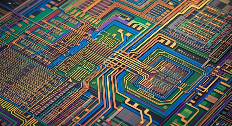
According to the strategy draft, MILM will provide the holding's enterprises with infrastructure for testing, certification, and reverse engineering of microcircuits, as well as for the analysis of chemical materials. PRTC, in turn, is to establish the production of photomasks—elements necessary for transferring the structure of a future chip onto a semiconductor wafer. The center is being established on the basis of MIET and is designed for the gradual mastering of photomask production with topological standards from 350 to 28 nm.
Photomasks: The Path to 28nm
The design capacity of PRTC will be at least 5,500 products per year with the possibility of increasing to 10,000. Mastering a wide range of topological standards—from 350 nm to 28 nm—will allow the center to serve different generations of production lines. In-house production of photomasks should reduce the dependence of Russian factories, including Mikron and NM-Tech, on foreign suppliers of this critical component.
Budget and Strategic Meaning
The total budget of the photomask center is estimated at least at 31.7 billion rubles: 24.3 billion is allocated by the Ministry of Industry and Trade, and another 7.4 billion was directed by Moscow for construction. The consolidation of production sites, testing infrastructure, and photomask production into a single holding, according to the authors of the strategy, will bring closer the creation of a full microelectronics cycle within the country—from materials and testing to transferring topology onto a wafer.