Hanwang Microelectronics has completed the installation of a second ASML lithography system at its facility in Liaoning Province, China. The equipment was delivered to the site of the 8-inch silicon wafer plant currently under construction, bringing the total number of lithography units installed on the production line to two. The company intends to bring the plant into full operational mode by the end of 2026, enabling the commercial production of high-tech components.
Project Scale and Investment Program
The Hanwang Microelectronics project involves a total investment of 3 billion yuan (approximately $415 million at current exchange rates) and spans an area of 375 mu—roughly 25 hectares. The facility is designed to develop and mass-produce MEMS (micro-electromechanical systems) chips for sensors. According to Chinese sources, the country currently faces a shortage of production capacity capable of high-volume manufacturing of such components, which underscores the strategic importance of the new plant.
Photolithography as a Critical Stage
The installation of both lithography machines formally completes the preparation of the photolithography area—one of the most critical stages in integrated circuit manufacturing. It is at this stage that the design of future structures is transferred onto the silicon wafer using ultraviolet light, determining the geometry and functionality of the final product. The enterprise can now proceed to the subsequent installation and tuning of auxiliary equipment, process verification, and preparations for the phased scaling of output volumes.
Management Stance and the Role of Partners
Huang Xiangxiang, President of Hanwang Microelectronics, stated that the company will accelerate the installation and commissioning of equipment, continue to refine manufacturing processes, and assemble a specialized team to support the technological cycle. In addition to the plant itself, the project involves ASML and other supply chain partners who ensure equipment integration and the transfer of technological expertise.
Local Government Support and Strategic Goals
Authorities in the Shenfu Demonstration Zone, where the project is being implemented, have expressed readiness to assist with the plant's launch, including equipment tuning and process optimization. The strategic goal of the project is to establish a major Chinese manufacturing base for MEMS sensors and strengthen the local semiconductor industry, aligning with China's broader objective to reduce reliance on imported components in technology-sensitive electronics sectors.
Context: ASML and the Chinese Market
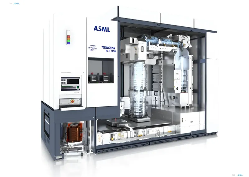
The installation of ASML equipment at the Chinese site confirms that, despite tightening export restrictions from the US and its allies, shipments of lithography systems to China continue within permitted categories. The TwinScan NXT:2150i model visible in the provided materials belongs to the DUV stepper class and is used in mature and sub-node process manufacturing, which meets the requirements for producing MEMS components that do not require extreme miniaturization but demand high precision in pattern transfer.