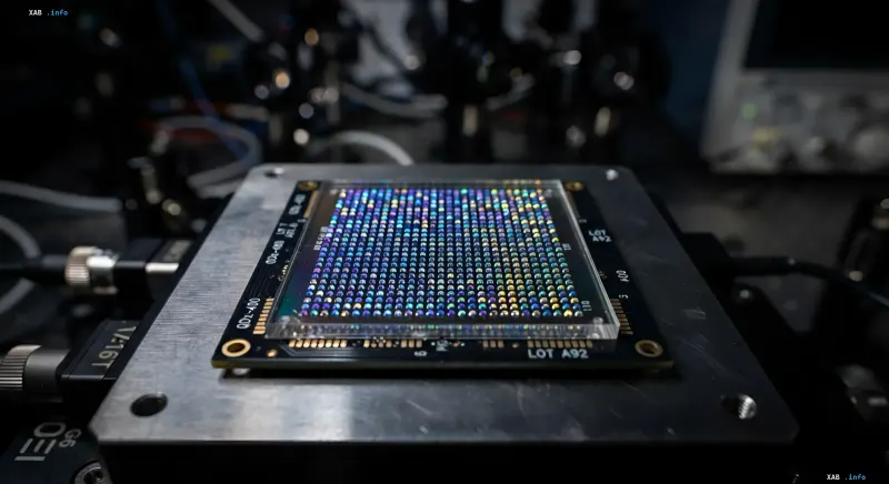
Researchers at Northwestern University (USA) have unveiled a platform they call the Megalibrary. On a glass substrate measuring just 2 × 2 centimeters, the scientists managed to place one million microscopic perovskite-type crystals. Each crystal is about 10 micrometers in size—tens of times thinner than a human hair—with all one million samples differing in chemical composition. The authors intend for this platform to test hundreds of material combinations simultaneously, thereby accelerating the discovery of promising substances for solar panels, LEDs, and semiconductor devices by many times.
How the 'Megalibrary' Works: From Polymer to Million-Fold Combinations
The chip fabrication technology is a multi-stage microfabrication process. First, the glass substrate is coated with a special polymer, in which a million microscopic indentations—essentially tiny "wells"—are formed. Then, researchers apply four different chemical solutions containing cesium, bismuth, antimony, bromine, and iodine in varying proportions to the surface. The substrate is then heated to 70 °C, and a crystal with a unique composition grows inside each well. As a result, one chip contains samples with a million different composition combinations—a quantity that would have previously required months of manual work in individual test tubes.
Unexpected Discovery: The Bandgap 'Breaks the Rules'
Working with the Megalibrary yielded a scientific breakthrough beyond the platform itself. Scientists expected that increasing the bromine content in the perovskite crystal would monotonically expand its bandgap—the typical behavior for most perovskite materials. However, the experiment revealed a different picture: the bandgap width first increased to 2.4 electron volts, then decreased to approximately 2.15 eV, and reached 2.11 eV in individual samples. This non-linear and non-intuitive path of optical properties required additional analysis of the internal crystal structure.
Shell and Core: Why the Crystal 'Behaves Strangely'
Detailed study of the internal structure revealed that the crystals form a two-layer architecture—a core and shell with different chemical compositions. The inner region concentrates bromine and antimony, while the outer shell is enriched with iodine and bismuth. These two regions have different atomic structures, which directly affects the material's interaction with light and explains the unusual change in optical properties. In essence, each crystal in the "Megalibrary" is a nanoscale heterostructural object rather than a homogeneous compound, opening up additional degrees of freedom when designing materials for specific optical tasks.
Durability and Limitations: What Doesn't Work Yet
The new material is not without flaws. During a ten-day test at a room temperature of 25 °C and 70% relative humidity, some crystal regions began to degrade. However, a protective polystyrene coating significantly slowed the degradation process, indicating potential for practical application provided additional encapsulation is used. It is important to note that at the time of the study's publication, the material had not yet been tested in actual solar cells or LEDs—this stage is about fundamental optical and structural characteristics.
Perspectives: From Accelerated Screening to AI Databases
The developed platform, according to the authors, allows for significantly faster screening of promising compounds and identifying internal structural features that cannot be captured when working with single samples. Future plans include using Megalibrary data to form structured databases, which will then be fed into artificial intelligence algorithms to predict properties of new materials. If this strategy is implemented, the "hypothesis-synthesis-testing" cycle in materials science could be reduced from months to days, which is particularly relevant for the renewable energy and optoelectronics industries, where demand for new perovskite and hybrid compounds is growing annually.