Samsung, having mastered manufacturing processes down to 2nm in recent years, is not abandoning its older 8nm node, which requires no expensive EUV scanners. The baseline variant—8LPU—was introduced back in 2017 and has remained in market demand ever since. Recently, the South Korean manufacturer announced an improved version of the platform, 8LPU+, which according to leaks will deliver up to a 12% performance boost, a 15% reduction in power consumption, and up to an 8% decrease in logic die area compared to the original 8LPU. Samsung intends to fully unveil the technology platform before the end of 2026.
DUV Instead of EUV: Hardware Cost Savings
The key distinction of 8LPU+ from Samsung’s modern 5nm, 4nm, and 2nm processes lies in its use of deep ultraviolet (DUV) immersion lithography to pattern critical layers. This allows the company to bypass purchasing extremely expensive EUV scanners, significantly cutting capital expenditures for production. Years of experience manufacturing 8nm chips gives Samsung a highly precise understanding of die yields and cost structures, simplifying financial planning and pricing for customers.
Target Segment: Reliability and Cost Take Priority Over Peak Speed
The new platform targets customers who prioritize low cost, high reliability, and long-term component availability over maximum performance. Expected application areas for 8LPU+ include automotive microcontrollers (MCUs), zonal control units (ZCUs), industrial robots, and edge artificial intelligence systems. In these segments, extreme lithography scaling requirements take a back seat to stability, thermal resilience, and extended support lifecycles.
Technical Features: eMRAM, ULL-SRAM, and 3.3V I/Os
8LPU+ features the integration of 3.3V planar input/output devices directly into the FinFET process, reducing the area of corresponding circuits by approximately 10%. To lower standby power consumption, ultra-low-leakage SRAM (ULL-SRAM) and high threshold voltage (cHVT) transistors are utilized. Special attention goes to the embedded magnetoresistive memory (eMRAM), which is traditionally in demand for automotive electronics due to its low sensitivity to ambient temperatures and high endurance of write cycles.
Exynos 9820 Die as a Reference
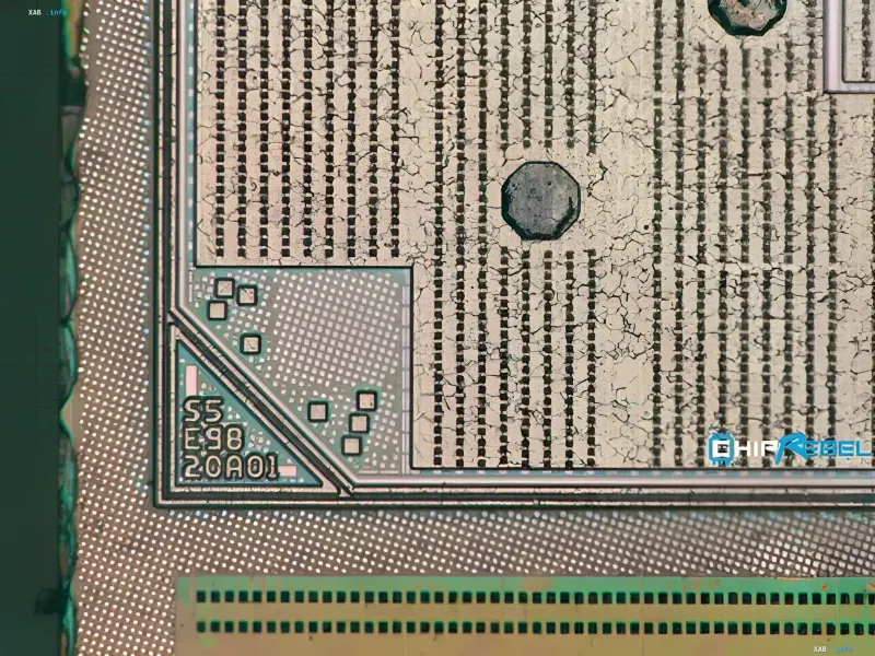
The illustration published by ChipRebel shows a fragment of the Exynos 9820 chip die manufactured by Samsung Foundry using the 8nm process. The image clearly displays characteristic rows of transistor structures, test pads, and marking elements, including the serial code "S5 E98 20A01". This die visually demonstrates the density and architecture of the logic blocks that will be optimized in the 8LPU+ version to reduce area and energy costs.
Caveats Regarding Figures
It should be noted that the specific figures—12% performance, 15% power reduction, and 8% area reduction—stem from leaks and have not yet been officially confirmed by Samsung in a press release. Furthermore, the industry typically improves one parameter while keeping another stable during a node transition, making simultaneous gains across all three directions less common. Final specifications will be revealed upon the platform's official launch, which, according to available reports, is scheduled for late 2026.