The global microelectronics industry is facing a new challenge that will radically alter the balance of power for decades to come. Dutch corporation ASML, the world's sole supplier of advanced lithography equipment, has officially adjusted its production plans. The reason is the integration of the ambitious Terafab project, implemented by Elon Musk in the USA, into the strategic delivery schedule.
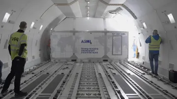
ASML's Chief Financial Officer, Roger Dassen, confirmed these changes during the financial results report for the second quarter of 2026. Deliveries of critical equipment will now be synchronized with the deployment stages of the Texas mega-factory. According to independent estimates, the scale of investments in this project could reach $119 billion by the time of full launch.
ASML's monopoly and the risk of shortage
Confirmation of orders from Elon Musk's structures has sent a signal to the entire industry. ASML holds a de facto monopoly on the production of extreme ultraviolet (EUV and High-NA EUV) scanners. Without these systems, it is physically impossible to produce processors using processes smaller than 5 nm. Traditionally, the queue for such equipment forms several years in advance and is distributed among giants like TSMC, Samsung, and Intel.
However, the emergence of such a major player as Terafab introduces corrections. According to EU antitrust legislation norms and WTO principles, the technology sector requires supply diversification. ASML's monopoly position creates a systemic risk: the market becomes "supply-limited." During periods of sharp growth in infrastructure projects from private investors, this inevitably leads to equipment shortages for the entire global industry.
Scaling capacity: figures and facts
In response to new challenges, ASML management announced a massive increase in target production volumes. The corporation plans an aggressive expansion of capacity over the next two years:
- Low-NA EUV systems: Base capacity, calculated for the release of about 65 units in 2026, will increase by 30% already in 2027. In addition, the possibility of additional expansion by another 30% in 2028 is being considered.
- Deep Ultraviolet Lithography (DUV): Capacity for the release of immersion systems (current level — around 130 units per year) will also grow by 30% in 2027 with the potential for similar growth in the following year.
The company's revenue forecast for this period is between €43 billion and €45 billion. ASML's capacity booking level is already close to 100%, and the Terafab project is already included in the portfolio of long-term orders.
Terafab architecture: vertical integration
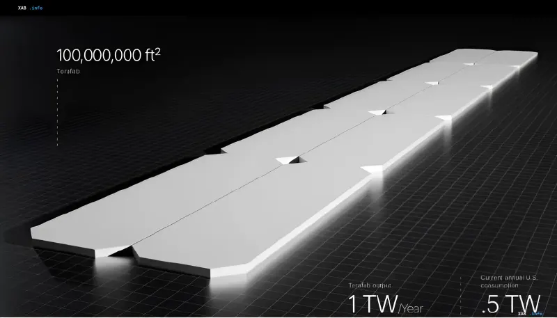
The Terafab project, developed by the Tesla, SpaceX, and xAI consortium, is based in Austin (Texas) near the Gigafactory Texas. The key industrial partner in the creation of the factory was the American corporation Intel. The main goal of the project is to eliminate a fundamental vulnerability of the modern IT industry: the geographical fragmentation of microchip production stages.
The Terafab concept implies full vertical integration of all cycles under one roof:
- Design and masking: Development of architecture for AI computing crystals and creation of photomasks.
- Lithographic casting (Fabrication): Direct production of logic integrated circuits on silicon wafers using ASML equipment.
- Memory release: Production of own high-bandwidth memory (HBM) modules, critical for AI computing.
- Final assembly: Integration of chips and memory into unified matrices and stress testing.
The ultimate goal of the complex's operation is declared to be the release of more than 1 terawatt of total computing power per year. This resource will be directed to equip Tesla autonomous systems, robotic platforms, as well as the creation of orbital data centers and supercomputers for SpaceX and xAI.