
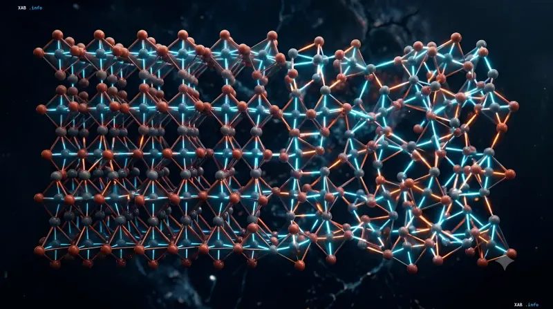
In August 2026, the scientific community focused on a fundamental discovery that could overturn the paradigm of microelectronics. Specialists from the University of California, Berkeley (UC Berkeley) and the Lawrence Berkeley National Laboratory (LBNL) demonstrated that titanium dioxide (TiO₂) — a material traditionally known as a standard dielectric — is capable of radically changing its properties when transitioning to the nanoscale.
The study, results of which were published in leading scientific journals, showed that at a film thickness of about 3 nanometers and less, TiO₂ begins to exhibit ferroelectric properties. Moreover, this effect does not disappear but rather intensifies as the thickness decreases to 1 nanometer. This discovery calls into question generally accepted views on the stability of material properties during miniaturization.
The Miniaturization Paradox: From Dielectric to Ferroelectric
Ferroelectrics are a class of materials possessing their own electric polarization, the direction of which can be switched by an external electric field. It is precisely this property that allows them to be used for data storage in non-volatile memory (FeRAM), where information is retained even after power is turned off. However, in classical solid-state physics, there is a rule: as the thickness of ferroelectric films decreases, their properties usually weaken or disappear entirely due to the so-called "dead layer effect".
Scientists from Berkeley decided to test the reverse scenario: can a material that is not ferroelectric in its bulk state acquire these properties precisely due to extreme reduction in thickness? The experiment confirmed the hypothesis. At a film thickness of about 3 nm, the crystal lattice of titanium dioxide begins to distort, its symmetry is disrupted, and atoms shift from their usual positions. This displacement leads to the emergence of switchable electric polarization — the main sign of a ferroelectric state.
Technological Breakthrough and Silicon Compatibility
Particular value is added to the discovery by the method of creating such films. Researchers used the atomic layer deposition (ALD) method, which allowed them to deposit TiO₂ directly onto silicon, silicon dioxide, and carbon surfaces at temperatures below 400°C. This is a critically important parameter for the modern industry, as it guarantees compatibility with existing silicon chip manufacturing technologies.
The most interesting observation was that the thinner the film became, the stronger the structural distortion manifested. The ferroelectric state was maintained even at a thickness of about 1 nm — this is effectively a layer of several atoms. For microelectronics, this opens the way to creating ultra-compact memory and logic elements that can switch at low voltages and consume minimal energy.
Prospects for Computational Logic and Memory
The potential application of this discovery is huge. Ferroelectric elements based on TiO₂ are being considered as the basis for a new architecture of processors and memory. Unlike modern DRAM, which requires constant power refreshing to hold a charge, cells based on the new effect will be non-volatile. This could lead to the creation of processors with instant startup and a radical reduction in the energy consumption of data centers.
Furthermore, the use of TiO₂ is an economically viable solution. It is a long-known, widely used, and well-studied industrial material. Its integration into production chains will not require the development of new chemical processes from scratch, which will significantly accelerate the path from the laboratory to the assembly line.
Contradictory Data and Implementation Challenges
Despite the optimism, experts point to a number of unresolved issues that create a certain uncertainty in estimates of commercialization timelines. On the one hand, laboratory tests confirm the stability of the effect at room temperature. On the other hand, there are concerns regarding the durability of the material under real operating conditions.
Researchers have not yet determined how many switching cycles (data write/erase) such an ultra-thin film will withstand before structural failure. Moreover, it is currently unclear whether the material will be able to maintain its unique properties as part of real transistors, where it will be subjected to high current densities and thermal loads. Some analysts believe that it will take at least another 5–7 years before commercial chips based on this principle appear, while optimistic forecasts from ALD equipment manufacturers allow for the appearance of prototypes as early as 2028.
Fundamental Science and the Search for New Materials
The discovery is significant not only for applied engineering but also for fundamental physics. It demonstrates that materials can radically change their electrical properties when transitioning to near-atomic thickness, violating conventional scaling laws. Scientists intend to use this principle as a new tool for searching for other substances capable of acquiring unusual properties when their size is significantly reduced, which could lead to the discovery of an entire class of future "supermaterials".