Samsung Electronics has officially finalized the architecture and production parameters for its new Fab 2 plant in Taylor, Texas. According to 3DNews, citing industry sources, the final decision on the plans was driven by two key customers for the future output: AMD and Nvidia. The plant will specialize in producing base logic dies for HBM4 memory—the logic chips that form the foundation of high-performance memory stacks used in artificial intelligence accelerators and big data processing systems. Samsung does not officially disclose client names or volume allocation ratios, but unofficial sources indicate that a significant portion of the production will go to AMD.
Scale and Technical Parameters of Fab 2
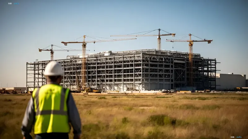
In terms of dimensions, the new plant will be approximately 1.5 times larger than the existing Fab 1 in Taylor, occupying around 250,000 square meters of manufacturing space. Fab 2 will be equipped with machinery to manufacture chips using a 2-nanometer class process node. The project timeline is as follows: major construction is set to begin in November 2026, equipment installation is planned for February 2029, and mass production is expected to kick off in 2030. For comparison, the neighboring Fab 1, which is already ready for full operations, began trial production of 2nm chips for Tesla, Broadcom, and Arm in September–October 2026, with mass production slated for 2027 at a capacity of up to 50,000 wafers per month.
HBM4 Base Logic: Why the Fourth Generation Changes the Rules
HBM base dies are logic microchips located beneath the vertical stack of DRAM dies. They handle memory management, data exchange with the GPU, and interaction with the accelerator's computing logic. However, starting with the fourth generation, the HBM architecture has undergone substantial changes: while previous base dies primarily managed memory functions, they now integrate more complex logic that can be tailored to specific accelerators. Future base dies for HBM4 will be significantly more complex than earlier generations, featuring specialized blocks optimized for the requirements of specific GPUs. Samsung is already using 4nm-class base dies for its HBM4 assemblies, combined with 1c-generation DRAM dies. According to the company, HBM4 delivers a data transfer rate of 11.7 Gbps per pin, with potential to increase to 13 Gbps, while a single stack bandwidth reaches 3.3 TB/s.
Open Question: Nvidia’s NVHBM and Samsung’s Stance
Uncertainty remains regarding the fulfillment of Nvidia's orders. Nvidia is promoting its proprietary NVHBM technology, which relocates part of the memory controller from the accelerator's main compute die directly into the HBM assembly's base die. According to technical data published by Nvidia, NVHBM will provide up to a 30% increase in bandwidth compared to standard HBM4E, reduce memory power consumption by 15%, and free up to 25% of the compute die area. TSMC has already expressed readiness to manufacture these controllers, whereas Samsung has not yet stated its position on this direction. Samsung will continue producing memory for HBM4 stacks at its plants in South Korea, and final packaging will likely also take place in the United States.
Strategic Shift: From Memory Manufacturer to Turnkey Solution Provider
Recent financial reports from Samsung show growing sales of HBM base dies and improved performance in its foundry division—a factor analysts believe influenced the decision to gear Fab 2 toward this specific product. Industry observers point to the possibility of expanding the supply chain through Broadcom, which produces AI accelerators for Google, OpenAI, and Anthropic. Altogether, Fab 2 in Texas represents part of Samsung's long-term strategy to transform from a traditional memory manufacturer into a turnkey solutions provider that combines semiconductor foundry services with advanced packaging. At the same time, experts remind us that by 2030, the U.S. semiconductor industry, according to projections by McKinsey and SEMI Foundation, will face a shortage of roughly 157,000 skilled workers, which could pose a risk factor for commissioning new capacities on schedule.