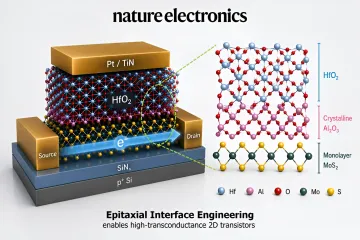
Taiwanese researchers, according to XBT.com, have reported the development of an ultra-thin buffer layer that could remove one of the key limitations of transistors based on two-dimensional semiconductors. The layer is made of aluminum oxide and is just 0.42 nm thick — a structure consisting of only a few atoms that allows an electrical insulator to be placed as close as possible to the conducting channel. In the experts' assessment, such atomic-level "primer" is a significant step toward atom-sized microchips, where controlling each individual atom at the material interface matters more than the choice of semiconductor itself.
Why Silicon Is Hitting a Ceiling
The miniaturization of traditional silicon components is gradually becoming a task of growing complexity: the physics and economics of the process are no longer scaling at the same pace. Against this backdrop, two-dimensional semiconductors — in particular molybdenum disulfide (MoS₂), whose thickness equals a single atomic layer — are being considered as a new alternative. In a conventional transistor, the gate controls the movement of electrons through the semiconductor channel, with a dielectric — an electrical insulator — located between them. The thinner this layer, the more precisely the gate controls the current, which is why the race to reduce insulator thickness has become one of the central directions in microelectronics.
How the "Primer" Solves the Interface Problem
The main practical difficulty with two-dimensional transistors is the defects at the boundary between two materials: they impede electron flow and noticeably degrade device performance. The proposed buffer layer addresses this challenge in two ways. First, it allows the main dielectric to be formed more uniformly and without pores. Second, the layer reliably protects the semiconductor channel from electrical defects. The experimental structure obtained during testing demonstrated good efficiency at a low level of leakage current, confirming the viability of the approach under laboratory conditions.
Contradictory Data
The available sources contain a minor discrepancy in how the facts are presented. The primary aggregator XBT.com explicitly points to the Taiwanese origin of the research, whereas specialized technology outlets covering the topic (including an article on "two-dimensional semiconductors as another approach to the problem") describe the breakthrough in general terms — as yet another step in the field of 2D transistors — without emphasizing the country or a specific laboratory. The numerical parameters (layer thickness of 0.42 nm, MoS₂ material, the requirement for ultra-high vacuum) match in both accounts, so the discrepancy concerns only the geographic attribution, not the technical essence of the result.
The Road to Mass Production
Despite its promise, the technology is still far from industrial deployment. The method requires transferring MoS₂ layers and processing them under ultra-high vacuum conditions, which complicates and increases the cost of production. In the experts' view, as transistors approach atomic dimensions, the decisive factor is not only finding suitable materials but also precisely controlling the boundaries between them at the level of individual atoms. This is why the atomic "primer" is seen as an infrastructural, rather than a final, element of future microchip architecture.