Amid the rapid depletion of the physical capabilities of silicon electronics, the semiconductor industry is seeking alternatives to continue Moore's Law. On August 9, 2026, a fundamental breakthrough was announced by researchers from National Yang Ming Chiao Tung University (Taiwan) in collaboration with TSMC engineers. The team developed a fundamentally new method for manufacturing transistors based on a two-dimensional material — molybdenum disulfide (MoS₂), which allows overcoming key barriers in current control and brings the technology closer to mass production of microchips.
The Interface Problem: Why 2D Materials Don't Work with Standard Insulators
For a long time, one of the main problems with MoS₂-based transistors remained the deposition of a gate insulator on them. The surface of a quasi-two-dimensional crystal has practically no free chemical bonds, making standard industrial methods, such as atomic layer deposition (ALD), inefficient. On such a surface, continuous ultra-thin films necessary for transistor operation are poorly formed.
Moreover, the use of high dielectric constant (high-k) dielectrics, such as hafnium dioxide (HfO₂), which is critical for miniaturization, enhances electron scattering. This leads to a sharp decrease in their mobility. Engineers had to find a compromise between carrier mobility and channel controllability, which inevitably led to deteriorated performance and increased defect rates.
The Solution: Epitaxial Interface Engineering and Atomic Buffer
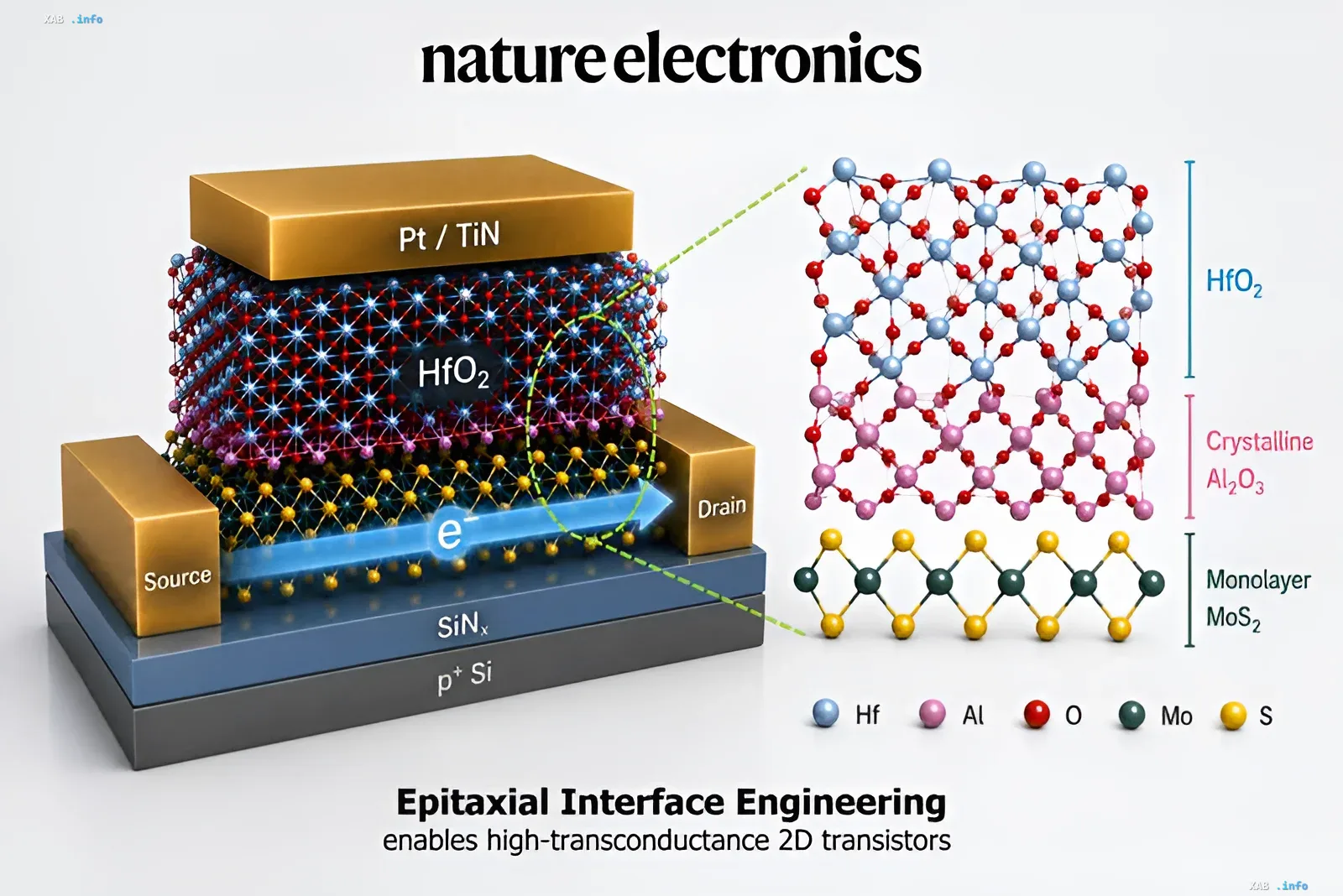
Scientists solved the problem by shifting the focus from searching for new materials to improving their joining methods. Essentially, they created an atomically thin buffer layer between the MoS₂ semiconductor and the main gate dielectric. Under ultra-high vacuum conditions, an aluminum layer about 0.3 nm thick was deposited onto the MoS₂ surface by electron-beam evaporation.
Thanks to the van der Waals nature of the 2D material's surface, the aluminum grew with the required preferred crystallographic orientation Al(111). After that, the layer was controllably oxidized, turning into an extremely thin and uniform layer of aluminum oxide (Al₂O₃). It was precisely this layer that became the key to success: it provided an ideal surface for the subsequent deposition of the high-k dielectric HfO₂ by ALD and simultaneously shielded the channel from unfavorable interaction with hafnium.
Results: Record Transconductance and Miniaturization
In the manufactured short-channel transistors, researchers managed to reduce the equivalent oxide thickness (EOT) of the gate dielectric to approximately 1 nm, without losing high carrier mobility. It is precisely the combination of these two characteristics that ensured the impressive transconductance of the electronic device.
This achievement is critical for further reducing the size of logic elements. Monolayer MoS₂ has a thickness of about 0.7 nm, allowing it to resist short-channel effects significantly better than silicon during aggressive scaling. The work demonstrates that one of the key barriers to 2D electronics — creating an ultra-thin gate without degrading the atomic channel — can be overcome through interface engineering.
Significance for the Industry: From Lab Experiment to Production
Although the work currently demonstrates a technological principle rather than a ready-made replacement for silicon CMOS processes, it paves the way for a new generation of chips. The created interface ceases to be just a mechanical spacer and becomes a vital functional part of the transistor. In the context of TSMC's current developments on processes below 2 nm, such technologies could become the foundation for the next generation of AI chips and high-performance computing.