#Semiconductors

News tagged with #Semiconductors

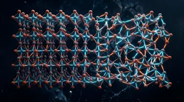
Atomic structure of titanium dioxide demonstrating quantum effects at one-atom thickness

Quantum Paradox: Titanium Dioxide Gains 'Superpowers' at One-Atom Thickness

Science 08/10/2026, 01:43
🔬 **Breakthrough in Microelectronics:** Scientists from Berkeley discovered that ordinary titanium dioxide (TiO₂) becomes ferroelectric at a thickness of less than 3 nm. 📉 **Effect Intensifies:** The thinner the film (down to 1 nm), the stronger the effect. This contradicts classical physics. 💾 **Future of Memory:** The technology will allow the creation of ultra-compact non-volatile memory and energy-efficient processors. ⚠️ **Challenges:** The durability of the material and the number of rewrite cycles are currently unknown. Years of research remain before mass adoption.
Read more →
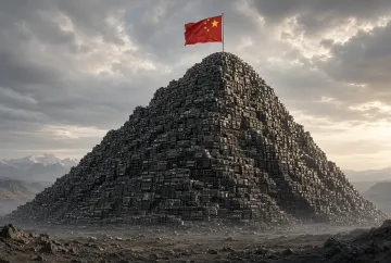
Chinese flag against a modern building, symbolizing the strategic shift to sovereign AI chips and advanced packaging

China's 'Big Fund' shifts strategy: from mass production to sovereign AI chips and advanced packaging

Technology 08/09/2026, 22:52
🇨🇳 China's "Big Fund" has moved to the third phase of financing, shifting focus to AI chips and advanced packaging. 📉 US sanctions pushed Beijing towards import substitution: in 2026, Chinese AI chips captured 79% of the domestic market. 💰 The fund supports companies like DeepSeek and SMIC, but analysts debate the effectiveness of investments under technological blockade. #China #AI #Semiconductors #Technology
Read more →
Dean Jarnak, new head of Intel sales, in a business suit on a white background

Strategic Realignment: Dean Jarnac from Marvell to Lead Intel Sales

Technology 08/09/2026, 21:19
🚀 Intel appoints new sales chief: Dean Jarnac moves from Marvell. He will take the post of EVP and be responsible for sales of AI chips, servers, and client solutions. Jarnac has over 30 years of experience, including work at AMD and Broadcom. He will start work in September 2026, replacing Greg Ernst, who is leaving after 27 years with the company. #Intel #Marvell #TechNews #AI
Read more →
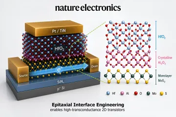
Schematic of a 2D transistor with epitaxial interface HfO2/Al2O3/MoS2 to prevent degradation

TSMC and Taiwanese Scientists' Breakthrough: How an Atomic Interface Saves 2D Transistors from Degradation

Technology 08/09/2026, 20:50
🚀 TSMC and Taiwanese scientists have made a breakthrough in 2D electronics! A new method for creating transistors based on molybdenum disulfide (MoS₂) has been developed. 🔬 The core problem: standard insulators are poorly deposited on 2D materials and reduce their performance. 💡 The solution: creating an atomic buffer of aluminum oxide between MoS₂ and the HfO₂ dielectric. 📉 The result: dielectric thickness reduced to 1 nm without loss of electron mobility. This opens the way to chips significantly more efficient than silicon counterparts. #TSMC #MoS2 #Semiconductors #TechNews #2DTransistors
Read more →
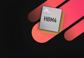
HBM4 memory chip from SK hynix, illustrating the news about espionage in favor of China

South Korea's Supreme Court Upholds Sentence for Former SK hynix Employee for Espionage in Favor of China

Technology 08/09/2026, 20:17
🚨 <b>Seoul Supreme Court</b> upholds sentence for former <b>SK hynix</b> employee for leaking secrets to China. 📉 In 2022, an employee transferred CMOS sensor data to a Chinese firm to secure employment. ⚖️ Sentence: <b>18 months in prison</b>. Appeal rejected. 🇰🇷 The case highlights the risks of industrial espionage in the semiconductor industry. #SKhynix #Technology #SouthKorea #Espionage #Semiconductors
Read more →
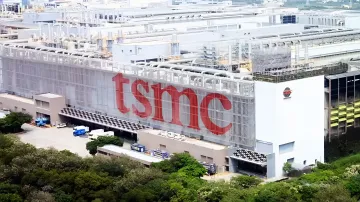
TSMC factory with red logo on facade, developing advanced 2D transistors based on MoS₂ in collaboration with NYCU

TSMC and NYCU Achieve Breakthrough in Microelectronics: New 2D Transistor Technology Based on MoS₂

Technology 08/09/2026, 18:31
🚀 TSMC and NYCU have unveiled a breakthrough technology for next-generation chips. Engineers have developed a method for creating 2D transistors based on molybdenum disulfide (MoS₂), which solves the problem of current control at the nanometer level. The key solution is the use of an ultra-thin aluminum oxide layer (0.42 nm) for ideal coverage. This could become the basis for processors with record density and energy efficiency in the coming years. #TSMC #Semiconductors #MoS2 #TechNews
Read more →
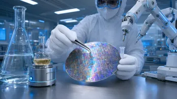
Engineer in a cleanroom inspects a silicon wafer with microchips using a robotic arm, symbolizing the launch of a new microelectronics certification system by the Ministry of Industry and Trade

Chemical Base Restart: Minpromtorg Launches New Certification System for Microelectronics

Technology 08/01/2026, 01:53
Minpromtorg of Russia has launched the development of a new certification system for microelectronics chemicals, allocating 54 million rubles for the project. 🧪🇷🇺 The goal is to move away from Soviet standards and create a base for import substitution by 2027. Plans also include a reform of localization assessment and the launch of production for 56 types of specialized materials. 📉🚀
Read more →